Capturing the Gameboy LCD with an FPGA (Part 1)


Update: see also Part 2.
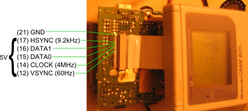
There are 6 important outputs from the Gameboy main processor to the LCD for capturing the pixels:
- Pixel data
D0andD1(50:LD0/DATA0, 51:LD1/DATA1) - Pixel clock
CLK(53:CP/CLOCK) - Line latch
CPL(55:CPL/DATALCH) - Horizontal sync
HSYNC(54:ST/HORSYNC) - Vertical sync
VSYNC(57:S/VERTSYN)
In brackets I've put the names and pin numbers for these signals from the
Gameboy schematic. You can tell these are the ones required as they are the
ones connected to the ICD2-R chip on the SGB (SGB schematic). Although only
D0, D1, CLK and CPL are strictly required.
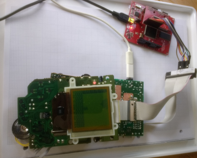
Don't forget that the Gameboy is 5 volt TTL: do NOT connect these directly to a non-5v tolerant input! I am using a Papilio Pro FPGA development board with an IO Buffer wing to handle the logic level conversion. I have soldered an old IDE ribbon cable to the pins of the ribbon cable which connects the main board to the LCD board of the Gameboy.
The pins to connect to are shown quite well in this image from the Nintendoscope project:
For testing I captured the signals using my Papilio Pro as a logic analyser with the Open Bench Logic Sniffer bitfile and sump-dump:
./sump-dump /dev/ttyUSB1 groups 1 trigger 0x20=0x20 divisor 10 vcd data=0x3 vcd clk=0x4 vcd hsync=0x10 vcd vsync=0x20 vcd cpl=0x40 vcd c=0x80
The signal buffer isn't large enough to capture a whole frame, it can only store about a third of a frame.


The behaviour of these signals is:
- Frame starts on the rising edge of
VSYNC, which is held high for the first line of the frame. - Each line of the frame starts on the rising edge of
HSYNC. - Pixels are generated from left-to-right from the Gameboy CPU.
- Pixel data is shifted into a 159 pixel (159x2 bits) shift register from
D0&D1on the rising edge ofCLK. - Note that
CLKdoes not run at a constant rate, some pixels are generated but the corresponding pulse ofCLKis suppressed so they are discarded. This is how the Gameboy implements fine (1-7) pixel background and window offsets (and possibly other effects). - A whole line of pixels is latched into the LCD drivers on the rising edge of
CPL. The pixels latched are the 159 from the shift register plus the values fromD0andD1(to make up 160 pixels). This also signals the end of each line, makingHSYNCa bit redundant. - At the end of each frame there are a few lines with no
CLKpulses but aCPLpulse, these don't have any effect on the display (as they will just latch exactly the same data into the LCD drivers each time). This could be used to detect the end of frame without having to useVSYNC. - In the logic captures I have looked at there is 160 rising edges of
CLK, so the first pixel generated (which always seems to be whenHSYNCis high) is actually discarded as it shifts off the end of the shift register before the row is latched into the LCD drivers.
The pixel data changes very soon after the rising edge of CLK for the next
pixel - so soon that to the logic analyser it appears to happen at the same time
as the rising edge. So I actually capture the D0 & D1 values from the cycle
before the rising edge is detected.
Capturing D0 & D1 on the falling edge of CLK seems to be widely reported
as the correct thing to do, but this will capture the whole frame shifted left
by one pixel. It is definitely easier though, so if you are happy with 159
pixels it is a decent approach.
Hardware
Used migen to build hardware, available here: gbcap. It's set up to build for the Papilio Pro, will require some changes to build with other FPGA boards.
This code sets up the pin assignment (from gbcap.py):
 plat.add_extension([
 ('gb_lcd', 0,
     Subsignal('vsync', Pins('B:5')),
     Subsignal('hsync', Pins('B:4')),
     Subsignal('cpl', Pins('B:6')),
     Subsignal('clk', Pins('B:2')),
     Subsignal('pixel', Pins('B:0', 'B:1')))])
i.e. D0 should be connected to pin 0 of the B wing header, and so on.
Once the bitfile is programmed onto your FPGA it will wait for a byte to be
received over the UART and then start capturing frames. You can grab these
using the recv.py script in the git repo, it will dump out pgm files.
The UART is only running at 2Mbaud in the current design, which is not fast enough to stream the Gameboy frame captures in real-time (that would require 60 * 160 * 144 * 2 = 2764800 bits per second), so you will only get a few frames before it stops due to FIFO overflow. Update: I now have real-time streaming, see Part 2.